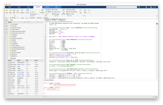
More work today and yesterday on this project. Still locking on 144 MHz, but this is normal, the crystal I used is a 48 MHz overtoned, working on the third harmonic in this case, thus spot on 144.0 MHz:
 I managed to clean the output, at the expense of transmitted power. I used a 7-pole 2m bandpass filter to tame the nasty harmonics and improve the spurious response. The output went down from +3.6 dBV (4.28 Vpp) to – 6.8 dBV (1.29 Vpp); on a 50 Ω load this translates in a decrease from apx 366 mW to 30 mW. However, the improvement in stability is impressive. I am not quite sure, though, if this is due to the notch filter or it is just a consequence of the reduced power:

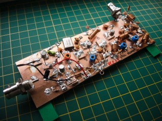
TX output. Spot on 144 Mhz, but this is after some mods that I did during past couple of days. Most importantly, I added a 7-pole Butterworth filter at the output, trying to tame the spurious response and some stubborn harmonics. Read on.
I’ve modified the schematic; from this:
 and some spare parts found in the junk box. At 7 dBV output (400 mW) Q2 is getting quite hot. Quite expected as these are not RF transistors. Capacitors labelled {C} are adjustable; had to use this symbol because the schematic is drawn in LTSpice that does not have a symbol for adjustable capacitors.")
The 144.8 Mhz TX Prototype schematic; a two-transistor TX, based on cheap components (2N2222) and some spare parts found in the junk box. At 7 dBV output (400 mW) Q2 is getting quite hot. Quite expected as these are not RF transistors. Capacitors labelled {C} are adjustable; had to use this symbol because the schematic is drawn in LTSpice that does not have a symbol for adjustable capacitors.
To this:
 is completely new.")
Modified schematic, indicating the AFSK insertion. The output filter (area highlighted in yellow) is completely new.
And it looks like that:

The three could in the filters are each 6 turns on a 5 mm rod, 1 mm enamelled copper wire.
The new filter is very effective. These were the results with the old schematic. Note the harmonics (hint: click on the images below to see animation in action):
 and velocity of each harmonic.")
FFT display of spurs and harmonics before changing the filter. Animated GIF. Each frame is delayed with 2 seconds, to allow display of measured values. Note the output (+ 3 dBV) and velocity of each harmonic.
Now, see the same analysis after changing the filter:
 and velocity of each harmonic.")
FFT display of spurs and harmonics before changing the filter. Animated GIF. Each frame is delayed with 2 seconds, to allow display of measured values. Note the output (-6 dBV) and velocity of each harmonic.
And another image without cursors:
 Interesting to note that crystal’s fundamental frequency (48 MHz) and all odd and even harmonics are well attenuated, but the filter has a less impressive effect on the 250 MHz, 375 MHz, 500 Mhz spurs. I am not sure what creates these spurs. Maybe they are a consequence of the prototype’s design (so called dead-bug) or maybe are induced by some other parasitic oscillations. One thing is certain, higher–level oscillations (aka spurs) are not related to my WiFi router emissions (somebody suggested this, so I wanted to rule it out). Or maybe there is a limit to the performance of this approach. I do believe, though, that I still have to dig and make some revisions of the schematic. However, I am satisfied by the results so far. The oscillations are stable and the waveform is clean, harmonics are well controlled and the carrier is locked well on my transceivers. For the sake of low–budget experiments with discrete components and with such a simple schematic, the transmitter behaves very well. I should probably add an LDO voltage regulator and stabilise the supply somewhere around 9 Vcc or maybe less. Curious what effect will this have upon oscillator’s stability (another suggestion that came from somebody else).
Next step will be to try some AFSK modulation. Stay tuned. More to come.

My small workplace with the scope in background and the new Fluke 289 on the right hand side.

144 Mhz TX. Carrier.