I am already one week into the design of the PCB for my new radio node and today I discovered some schematic errors that I had to fix. Running the DRC (Design Rule Check[er]) KiCad threw some schematic parity errors which “occurs when there’s a mismatch between the schematic diagram and the physical PCB (printed circuit board) layout, indicating a discrepancy in the design…” (Google AI). In this context, parity refers to the consistency or matching of design elements between the schematic and the PCB. In some less academic wording this means that any symbol in the schematic should have a footprint corresponding to in the PCB.

This comes when I added some graphic elements as footprints on my back silkscreen layer and, since PCB editor is expecting a corresponding symbol in the schematic, the eror is thrown. This normally does not happen if you use graphic files and import them directly into the silkscreen layer, but I find this method quite unreliable. First you have to 1/ create a horizontally flipped graphic otherwise will not show properly on the back silkscreen layer and 2/ to tweak the scale at the import, which is always a trial-and-error process. I did not find a way to have the same scale harmonized between my vector graphic software and KiCad. Read more.
Thus, I prefer creating footprints of various sizes using KiCad’s Image Converter snippet, from same bitmap or vector graphic. Then I place them directly on the silkscreen layers. The system will take care of flipping depending on the chosen side. However, this method always generate these schematic parity errors.
To mute them you either have to create a corresponding symbol and place that on the schematic or add these warnings to the exclusions list in DRC:

Excluding a violation in Design Rule Check, KiCad. I personally do not like this approach because it is very easy to add by mistake an exclusion for otherwise useful warning or error.
I chose creating symbols and adding them to the global library. I created one symbol for each graphics that I need. Later, I can choose the size of the footprint depending on the design. I can use KiCad’s Image Converter anytime to generate any number and any size of footprints that can be attached to the graphic symbols depending on the need of my design.

Various graphic symbols created in KiCad Symbol Editor and assigned to footprints in PCB Editor. This will remove the Schematic Parity warnings.

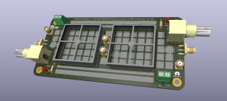
The end result: PCB with graphic footprints
This concludes another endeavour in the wonderful world of KiCad. Stay tuned. 73