PCB design and pick and place issues

How to avoid pick and place coordinate offset in KiCad


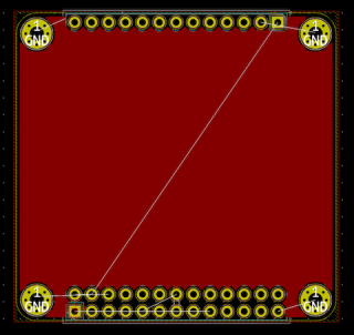
There is a problem (or I am doing something terribly wrong !) with the coordinate system in KiCad.

When exporting fabrication outputs for pick and place, make sure you deselect the “Use drill/ place file origin” from the dialog window. For me this worked best and avoided any issues I got from JLCPCB online quote tool regarding placing components.

Even if I selected the bottom left corner of my board as origin for drill files, it did not work correctly and I got an offset when uploading the CPL file to JlCPCB:

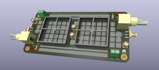
This is a rendered image of the correctly placed components by not selecting the “Use drill/place file origin” option:

Categories: Electronics, PCB Development Tags: ,

Raspberry Pi compatible, SA818 radio node

My new radio node that I designed last month is back from production at jlcpcb. Designed in Romania and built in China 😁. This is my first attempt using jlcpcb for the entire manufacturing chain, from PCB creation to part selection and assembly.

Schematic Parity Error

I am already one week into the design of the PCB for my new radio node and today I discovered some schematic errors that I had to fix. Running the DRC (Design Rule Check[er]) KiCad threw some schematic parity errors which “occurs when there’s a mismatch between the schematic diagram and the physical PCB (printed […]

Comments are closed.